Optimized Reflow Profiling to Minimize Voiding
By MB Allen, Manager, KIC
In this whitepaper we discuss several aspects of the challenges of PCB voiding with bottom terminated components (BTCs). This includes what voiding is, the causes and its effect on components. We will look at the challenges and some solutions, primarily solutions that focus on thermal profiling. Additionally, we will explore the tools that you may already have, those that are available to you right now, and how to improve your knowledge base regarding thermal profiling issues.
The PCB Voiding Challenge
Voiding has been a challenge for quite some time, primarily with BGAs, ever since the shift to lead-free soldering was discussed in the United States. It continues to be a problem for lead-free assemblies, but the problem has become even more complex.
With miniaturization and many BTCs we continue to struggle to find the true causes and the ideal solutions. In addition, the change in PCB (printed circuit board) assemblies is incredible. Some assemblies seem to ignore any DfM (Design for Manufacturability) rules. They vary from small PCB assemblies with miniaturization of parts and often a BGA to very large, heavy double-sided PCB assemblies with ground planes, heat sinks, and densely populated. Added to that, the mixture of circuit board components from those which cannot be seen with the naked eye to tantalum capacitors, BGAs, QFNs, plastic connectors, shields and much more.
The next challenge is the reflow process window. Typically, the process window is focused around the solder paste, but often some components cannot accept the temperature tolerances of many lead-free solders.
‘Whether for power electronics, electronic aviation systems, medical equipment or electronic systems for the automotive industry, solder joint voids represent a significant problem. Enclosed voids can cause for displacement of electrical and thermal paths as well as local concentration of power and heat.” Markus Walter, Seho
We deal with the problem of voiding during manufacturing yet it’s the final effect on a product that is the key, sometimes that gets lost. That is why voiding is such an important issue.
The Cause of PCB Voiding
Voiding is attributed to the flux outgassing within the solder joints when the solder is at a molten state.
Potential Solutions to Reduce PCB Voiding
One of the biggest advancements has been changes to solder paste chemistry. However, making a change to a new solder paste is not a ‘drop in’ solution nor is it always the correct solution. Often a contract manufacturer is given specific materials to use when assembling a board, so they can’t just change the paste without a new qualification process, which let’s face it, is costly and time consuming. Add to that, while this material may solve the voiding issue for some components, it may cause problems elsewhere on the circuit board. Many companies don’t want to have multiple solder pastes and often a low-voiding paste is not the correct solution for all assemblies. Thus, changing materials may not be ideal, or even a possible, solution.
Then there is the PCB stencil. I have seen some incredibly creative stencil apertures to adjust the amount and spacing and amount of the paste deposition. This is a possible solution. However, trying multiple stencils is costly and time consuming too. Trial and error seldom feel like a good solution. Placement is also a key element in the voiding problem and an important place to look for problems.
Another solution may be a new type of reflow oven, specifically a vacuum reflow or ultrasonic reflow oven. This is an expensive solution and may be hard to justify. Typically, we see factories invest in one of these ovens for specific products with void-susceptible assemblies.
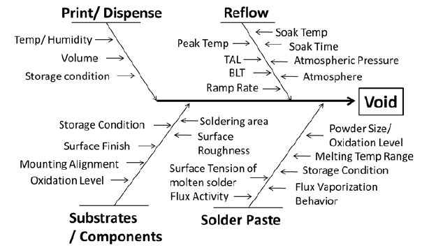
Having gone through all the above potential solutions what’s left? In short, the thermal profile! And the best news about this is that it’s an immediate fix. Even if you’re going to experiment, you can see the results and make decisions quickly, so more uptime, and greater cost savings.
Above is a chart of factors that impact voiding. With respect to PCB reflow we should focus on Peak Temperature, TAL (Time Above Liquidus), Ramp Rate and Soak Time. These are the key areas of the thermal profile that can be changed to reduce voiding.
Even when focusing on the thermal profile there are yet more challenges. Exactly what to change is based on the PCB density and components, finding a balance to fix one area without impacting others. One example is the LED. Some suggestions for reducing voiding in LED assembly is increased temperatures, which can be harmful to LEDs. Too much heat can cause changes in the LED’s luminosity, thereby changing the final product. LEDs can be expensive, so special attention must be given to them.
The Art of Thermal Profiling
“.. the profiling process remains primarily as an art. Improvement in voiding control often comes out as results of extensive trial and error. Apparently, a fundamental understanding of the effect of the changing profile on voiding becomes critical for a prompt and efficient voiding reduction.”
Dr. Yan Liu, Dr. Ning-Chen Lee et al, Indium Corp, reference ‘A Model Study of Profiling….” See ‘References 2’
“Profiling is the only real-time input variable that affects outcomes.”
Tim O’Neil, AIM
To find the right PCB profile it is key to focus on these areas of the thermal profile.
- Soak – There must be a balance between a too slow soak (avoid oxidation) and a too fast soak (entrapping the volatiles). For the most part a ‘soak’ profile is no longer commonly used when having a problem with voiding.
- The Ramp to Peak, also known as Tamp to Spike – Tent and/or Straight Ramp (depending on the solder paste company) is that which is currently being used to reduce voiding. There are two different schools of thought on this. One in favor of a lower peak and one in favor of a higher peak, the greatest consensus being the higher peak.
- Ramp Rate is also a key, concentrating on the amount of time and rate at which the activation takes place and the volatiles are released.
- Time Above Liquidus (TAL) is a key to improved wetting, less chance of flux entrapment.
- TAL and peak are two areas where there are the majority of changes to the profile, and therefore time given to experimentation.
As we progress with these changes to the profile we MUST consider the rest of the PCB assembly. Temperatures that are too high can cause damage to parts like plastic connectors or LEDs. Thus, when setting up a recipe for a thermal profile it is imperative to find a solution that gives you a reliable solder joint for the entire assembly, this is the biggest challenge. It is recommended to attach thermocouples (TCs) to all the critical components for a good representation of the printed circuit board.
Many people will drill below a Ball Grid Array, for example, and attach a TC at the ball. This is, of course, the most accurate method of knowing exactly the temperature of the solder paste but not always possible.
There are solutions available for non-destructive thermal profiling, for example, using aluminum tape for TC attachment. There is a paper from Rochester Institute of Technology (RIT) on a study specific for non-destructive profiling on BGAs. They have created a ‘calculator’ so you can attach a thermocouple on top of a BGA that calculates the temperature at the ball.
Void Avoiding Profiling
Process Window – Increased Soak Temperature

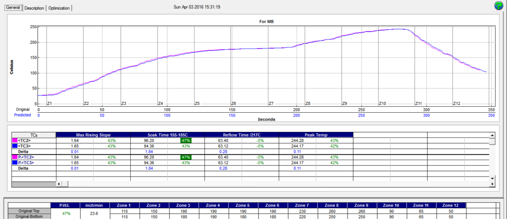
While I mentioned that generally a reflow profile with a soak is not recommended when trying to reduce voiding, for those wishing to maintain a soak, our research shows that the soak process window should go up to 200C. The range in this specification is 155-185°C. Thus, this would be changed to 155-200°C (Figure 1.).
Below (Figure 2.) is a view of a reflow soak profile commonly used for lead-free solder manufacturing.
To maintain a soak profile this would be changed as indicated in Figure 1. to increase the process window soak temperature to 155-200C.
Process Window – RTS (Ramp to Spike)
Now we consider the ramp to spike/peak. Again, this is a sample of a common process window for LF manufacturing. Note the temperatures and TAL (Figure 3) and the resulting profile (Figure 4).


Process Window – RTS Long TAL, High Peak
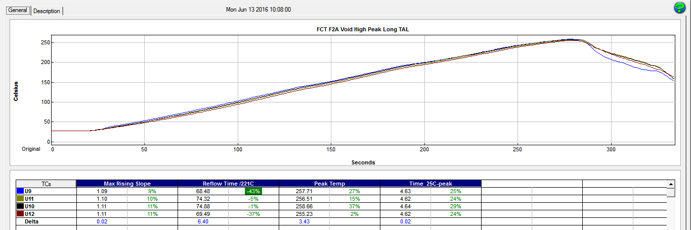
In this case, a longer TAL and higher peak temperature is used to reduce voiding.
There is an increase in the TAL from 45-75 seconds to 60-90 seconds (Figure 5.). In addition, there is an increase in the peak temperature from 235-255°C to 245-265°C. There should be caution given to this process window because this is getting close to some component’s maximum temperatures. There are variations of this of course, a slightly lower peak and a shorter TAL, like 255-259°C and TAL of 68-75 seconds but these create very tight process windows. The resulting profile is shown in Figure 6.

Fine-tuning – The devil is in the details
Fine tuning can take time, but you can see the result immediately. Using tools available on the market for this optimization process significantly reduces the amount of time needed, including the amount of trial and error thermal profile runs. These are inexpensive and can save you so much time, money and stress.
I mentioned earlier the importance of attaching thermocouples to all the critical components and a good representation of your board. ‘Location, location, location’ is not just important when finding a new home but also when establishing a profile. Once again, software is available to assist with this.
KIC offers a unique software solution. When you attach a thermocouple to a particularly difficult and/or sensitive component you can create a specific process window for it. This may be a subset of your ‘solder paste spec’. You may have attached TCs to several parts that use the solder paste spec but for your QFN, plastic connector, LEDs, you may set up a separate process windows based on the component spec. The best part of this is that our software will display the results, including KIC’s Process Window Index, for each of the individual TCs attached to the components. And when the software optimizes for the best recipe, it takes each one’s individual process window into consideration and suggest the best recipe for the entire assembly.
Profiling – Oven Changes, Optimization and more
The two most common settings for establishing a recipe for a good reflow profile are the zone set-points and conveyor speed. In software you can easily control what you may or may not want to change, including optimization with the fastest belt speed for higher throughput or least amount of zone set-point changes for faster changeover. Figure 7. shows oven zone setpoints and conveyor speed changes automatically suggested by optimization software for a recipe that generates an in-spec profile. You will notice that there is no soak in this, i.e. an RTP.
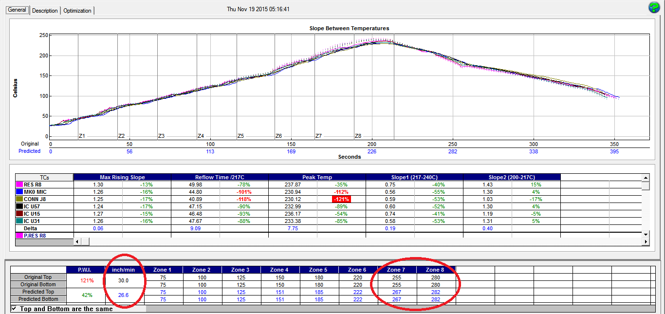
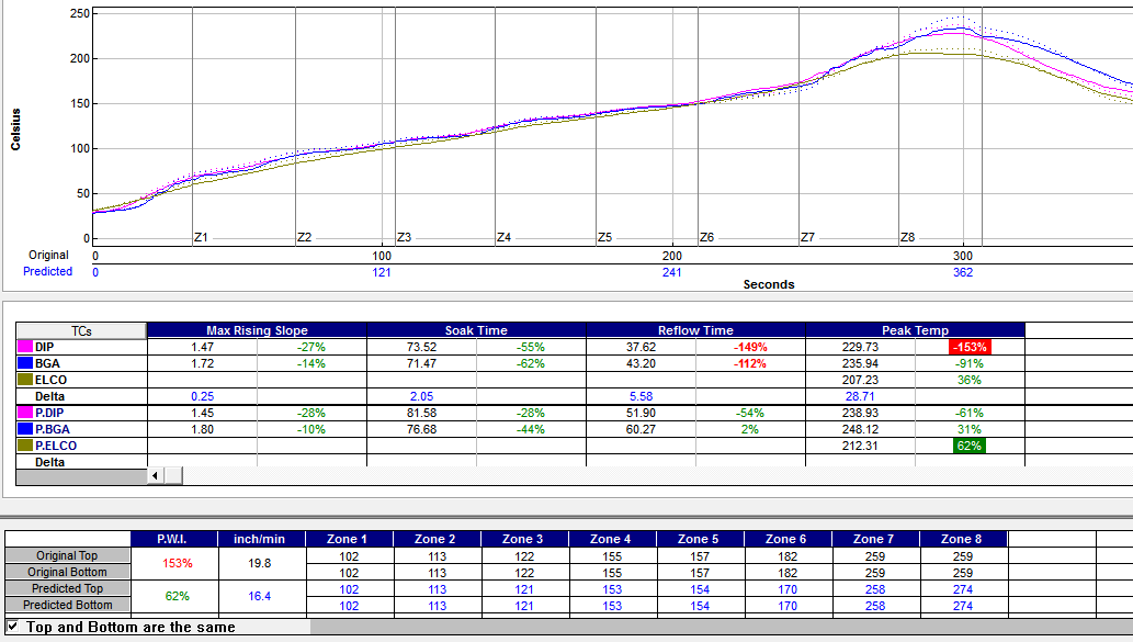
Separate Specs By TC – Create a separate process window for each component with a TC attached.
Having the ability to build a reflow profile around the entire populated PCB is critical to achieving the solder paste recommendations, maintaining the component specifications and reducing voiding. Below each thermocouple’s results are shown as they relate to each of their designated process windows (Figure 8). The quick tool of establishing a process window for each TC/component will force the automated prediction software to look for an oven recipe that results in an in-spec profile for all the TCs are within their respective individual process windows, saving time and money.
Knowledge is King
The fastest and easiest way to optimize a PCB profile for void reduction is with knowledge. Too often people have a voiding issue, call their solder paste company and when asked what the thermal profile is, the response is ‘I didn’t profile’. You cannot get a resolution for a problem if you have no information. Can I stay below 65 MPH in my car without a speedometer?
Analyze the layout of your printed circuit board assembly. Know where the ground planes are, where there are top and bottom components with different heat tolerances and so on. Know your oven’s capabilities and its limitations. If you’re trying to reflow a lead-free assembly with a densely-populated board for a backplane you may not have the correct oven.
Again, look at the big picture.
“Soak profiles are commonly used to help equalize temperatures across the circuit board. Soak profiles are also recommended for certain solder pastes to drive off volatile materials and to fully clean and activate the metal surfaces. Extended soak times and/or high soak temperatures can cause pre-mature loss of activity in the solder paste resulting in wetting and solder balling issues.
Linear ramp to spike profiles are also commonly used and are typically a good starting place for most SMT processes. Linear ramp profiles provide enough time for the solder paste to activate and clean the metal surfaces while minimizing the risk of pre-mature loss of activity. The addition of a short soak can minimize the potential of defects like tombstoning. This needs to be done in a specific manner for each solder paste, because each solder paste responds differently to these type of profile changes.” Tony Lentz, FCT Assembly.
Tools & Self-Help
Most people already have thermal profilers in their factory, so use them. Know what features the software offers and how best to use it. Ask your thermal profiler supplier for assistance and see what’s new and available.
Sharing is Important
Some of us are getting older yet have years and years of experience. Much of that knowledge is in our heads. We need to share this knowledge. My suggestion is to implement a system (knowledge library) internally to document things, problems that you’ve found solutions for, more efficient ways of doing things, etc. If you’re out on vacation and a problem arises that you spent quite some time finding a solution for, let that be known in a ‘reference guide’ so the person now trying to find the solution doesn’t have to start from scratch and waste all that time again. Share your knowledge, it’s very important to your company AND will save money.
Conclusion
• Key focus to reduce/eliminate voiding is the reflow profile
▫ Longer TAL
▫ Higher Peak Temperature
• Solder paste specifications are a GUIDELINE only.
▫ It is imperative that you take the entire assembly into consideration when establishing the correct recipe for the profile you want to achieve.
Excerpt from Aim Reflow Profile Supplement:
“The information provided is a guideline only. Your profile will depend upon many factors including paste chemistry, customer requirements, component limitations, oven characteristics, board layout, etc. Ultimately, quality requirements should drive the process, not adherence to these guidelines.”
- Fine-tuning a profile for specific components limitations should be considered
- Include TCs on void-susceptible components when profiling
- Balance TCs across components and PCB challenges
- Use available tools to improve the time and accuracy of finding an optimum profile
- Some of these tools you may already have and not even know it, others are inexpensive and can ultimately improve the time and accuracy of finding the optimum profile.
References:
- An interview with Markus Walter, CEO of Seho Systems GMBH. SMT Today, November 2015 issue.
- A Model Study of Profiling for Voiding Control at lead-free Reflow Soldering, by Dr. Yan Liu, William Manning, Dr. Benlih Huang, Dr. Ning-Cheng Lee, Indium Corp.
- Fill the Void by Tony Lentz & Greg Smith, FCT Assembly.
- Controlling Voiding Mechanisms in the Reflow Soldering Process by Keith Sweatman, Takatoshi Nishimura, Kenichiro Sugimoto, AKira Kita, Nihon Superior Co., Ltd.
From the July / August 2019 issue of SMT Today magazine
https://kicthermal.com/wp-content/uploads/2019/03/Optimized-Reflow-Profiling-to-Minimize-Voiding.pdf
